3D Systems trending up
3D Systems Corporation (DDD) trend seems to continue up on the short and long term.
The 3d Printer hype still looks quite strong.

Labels: 3d printing, DDD, nanotech
posted by GM @ 11:54 AM
0 comments


3D Systems Corporation (DDD) trend seems to continue up on the short and long term.
Labels: 3d printing, DDD, nanotech
posted by GM @ 11:54 AM
0 comments
PowerShares Lux Nanotech (ETF) is one of the few 'true' nanotech ETF.

Labels: nanotech, Nanotech ETF, PXN
posted by GM @ 4:54 AM
0 comments
Display technology is currently realizing the benefits of nanotechnology in lighting support for the displays and the display construction itself.
Display technology is currently realizing the benefits of nanotechnology in lighting support for the displays and the display construction itself. One of the new display technologies is the Mirasol display from Qualcomm. This MEMS (microelectromechanical-system)-on-glass device targets low-power, daylight-readable color displays for portable-system applications.
Most LCD devices operating at low power, such as with mobile phones and tablet PCs, have issues with color representation. In varying light, the color accuracy of the display changes, altering the viewer’s perception of the image. The Mirasol display attempts to overcome these issues.
The display is a front-reflective display rather than a traditional backlit display. The properties of nanoscale materials combine with advanced MEMS-processing techniques, allowing the display to mimic naturally occurring phenomena. The display works by creating a color from an interference pattern on the reflected light that hits the top of the display. This process is the same one that makes a butterfly’s wing shimmer and display different colors.
Labels: Nano news, nanotech, nanotechnology
posted by Ertai @ 8:10 AM
2 comments

A new anti-reflective coating developed by researchers at Rensselaer Polytechnic Institute could help to overcome two major hurdles blocking the progress and wider use of solar power. The nanoengineered coating boosts the amount of sunlight captured by solar panels and allows those panels to absorb the entire spectrum of sunlight from any angle, regardless of the sun's position in the sky.
An untreated silicon solar cell only absorbs 67.4 percent of sunlight shone upon it — meaning that nearly one-third of that sunlight is reflected away and thus unharvestable.
After a silicon surface was treated with Lin's new nanoengineered reflective coating, however, the material absorbed 96.21 percent of sunlight shone upon it — meaning that only 3.79 percent of the sunlight was reflected and unharvested. This huge gain in absorption was consistent across the entire spectrum of sunlight, from UV to visible light and infrared, and moves solar power a significant step forward toward economic viability.
Labels: nanotech, nanotechnology, Solar Energy, Solar Nano
posted by Ertai @ 12:30 PM
3 comments

If you thought nanobots might give us cause for concern when the singularity occurs, how about nanobots made from DNA? U.S. scientists have developed microscopic robots composed of DNA that can follow instructions and work together like an assembly line to make products such as particles of gold.
Reporting in the journal Nature, New York University chemistry professor Nadrian Seeman and colleagues describe a tiny DNA factory consisting of a DNA track for assembly, three molecular forklifts that can deliver parts, and a DNA "walker" that moves around like a car on an assembly line.
The team had produced the first such DNA walker in 2004, knitting together strands of DNA to form a mobile molecule. With the walker working in the nano-factory, the plant can be programmed to produce up to eight different combinations of gold nanoparticle chemical species, according to the researchers.
Labels: DNA, nanofactory, nanotech, nanotechnology
posted by Ertai @ 3:25 PM
1 comments

All our modern technologies from information and communication, energy, and the environment to health and transport depend on the development of materials that can withstand the highest mechanical and thermal load, transfer data at the greatest speeds, safely store data in the smallest dimensions, ensure biocompatible transplants, remove monoxides from car exhausts, or separate protons and electrons in fuel cells.
This has led to great expectations for the future of nanomaterials science and worldwide attention has been drawn to the enormous potential of nanoscience and nanotechnology.
Although Europe’s expertise in nanomaterials science is excellent, it is highly fragmented into scientific disciplines, sectors and national efforts which are on a global level often subcritical. Europe would considerably benefit from a strategic pan-European, multidisciplinary research involving all sectors and the most advanced European research infrastructures.
Labels: Nano news, Nano RD, nanotech, nanotechnology
posted by Ertai @ 5:55 AM
0 comments
DTU Nanotech is the Department of Micro- and Nanotechnology at the Technical University of Denmark.
Labels: nanotech, nanotechnology
posted by Ertai @ 11:46 AM
0 comments
The 50 day Moving Average is now above the 200 day Moving Average, near a crossover, the short-term chart looks like this:

Labels: Nano Tech Stocks, nanotech, Nanotech ETF, Nanotech stocks, PXN
posted by Ertai @ 6:52 AM
0 comments
Tiny semiconductor particles known as "quantum dots" have been used in a sensor that could make for mobile phone cameras that outperform larger cousins.
A film made from these dots is more light-sensitive than existing approaches to camera sensors, according to its makers, Invisage.
That means that cameras made using the film need not be as large as some to achieve the same performance.
InVisage suggests the films will make it into camera production by mid-2011.
Digital camera sensors rely on silicon to do the crucial business of turning incoming light into an electric charge that the camera can measure and translate into an image.
But the way silicon-based sensors are produced means that in many cases the light is partially blocked by the electronic connections that make the sensor work.
Combined with the fact that silicon can turn only half of the incident light into electric charge, capturing light using silicon throws away about 75% of the light.
Labels: Nano news, nanotech, nanotechnology, Quantum dots
posted by Ertai @ 8:37 AM
8 comments
PowerShares Lux Nanotech (ETF) is one of the few 'true' nanotech ETF, even if most companies aren't tied to just nanotechnology business, in the long term future some of these companies might be the ones to grab the emerging technology of the nano-scale.

Labels: nanotech, Nanotech ETF, Nanotech stocks, nanotechnology, PowerShares Lux Nanotech, PXN
posted by Ertai @ 10:53 AM
0 comments

Imagine a world where sunlight can be captured to produce electricity anywhere, on any surface. The makers of thin-film flexible solar cells imagine that world too. But a big problem has been the amount of silicon needed to harvest a little sunshine.
Now, researchers [led by Harry A. Atwater] at Caltech say they’ve designed a device that gets comparable solar absorption while using just one percent of the silicon per unit area that current solar cells need. The work was published in the journal Nature Materials.
The research team tried silicon wire arrays instead of traditional silicon panels. These wires have been shown to do a good job converting sunlight to usable energy on the nanoscale. But the scientists had to create wires a thousand times longer.
Light bounces around within the wires and is eventually absorbed when it hits at the correct angle. But there was a problem: too much light was leaking out. Adding nanoparticles of alumina kept much more of the light scattering until it got absorbed. The result is a system that virtually matches silicon wafer light absorption and may be more efficient at converting light to electricity, while using a tiny fraction of the material.—Cynthia Graber
Labels: nanotech, nanotechnology, Solar Energy, Solar Nano
posted by Ertai @ 8:12 AM
3 comments
A report in the journal IEEE Transactions on Nanotechnology shows that maple trees generate a small, but measurable amount of electricity, which can power tiny devices. Karen Hopkin reports
If scientists have their way, we may someday be tapping maples—not for pancake fixin’s, but for power. Because researchers from the University of Washington in Seattle have found there’s enough electricity flowing in trees to run an electronic circuit.
If you’ve ever made a potato battery, you know that plant material can generate current. But the energy in trees is something else entirely. The potato experiment uses electrodes of two different metals to set up a charge difference that gets local electrons flowing.
But in the current study, researchers use electrodes made of the same material. Sticking one electrode into a tree and another in the soil, they found that big leaf maples generate a steady voltage of up to a few hundred millivolts. That’s way less than the volt-and-a-half provided by a standard AA battery. So the scientists designed a gadget so small, with parts just 130 nanometers in size, that it can run on tree power alone.
Labels: Nano news, nanotech, nanotechnology
posted by Ertai @ 5:07 AM
9 comments

A team of British researchers are set to begin a trial program by planting nanotechnology-based artificial arteries into humans.
Scientists at London's Royal Free Hospital received a grant of more than $800,000 to move the artificial artery project from the laboratory to human trials within the next year, according to the hospital. The artificial arteries are made of a polymer material that's combined with nanomaterials. The hospital said the materials can closely mimic natural vessels by pulsing along with the beating of the patient's heart.
The grant was issued by the Wellcome Trust, which is the largest charity in the U.K.
"The new micro-graft pulses rhythmically to match the beat of the heart," said George Hamilton, a team leader and professor of vascular surgery at the Royal Free Hospital. "As well as this, the new graft material is strong, flexible, resistant to blood clotting and doesn't break down, which is a major breakthrough."
The arteries are designed to replace ruptured or diseased vessals in human hearts and legs.
Nanotechnology has been a major part of medical research in recent years.
Labels: Nano news, nanotech, nanotechnology
posted by Ertai @ 6:07 AM
9 comments
It's a battery made out of coated paper.
Labels: Nano news, nanotech, nanotechnology
posted by Ertai @ 2:27 PM
2 comments
RUSSIAN pledges to spend billions in public funds to develop its nanotechnology industry are being treated cautiously by leading British technology companies.
President Dmitry Medvedev said the country will channel 318bn rubles (£6.3bn) into the development of a nanotech infrastructure to increase exports of products built in Russia using the technology.
Oxford Instruments, a British nanotechnology company, said, however, that that it may take time for the cash to become available.
Frazer Anderson, a business development director, from its Bristol-based plasma technology division, said: "Their timescales are a lot longer than ours. If they say $10bn, they probably will do that over the next 10 to 15 years." He added: "If you see big numbers it's excellent but the reality is that it does not always come to pass."
However, Mr Anderson said his company had seen an increase in technology spending from governments worldwide as part of their fiscal stimulus packages.
"We do see President Obama putting more into solar and solid-state lighting. We see that in China. India is on photovoltaics," he said.
This trend had led to more demand for Oxford's equipment. The technology is used to create thin-film or nano-tech devices in everything from the motion sensors in the Nintendo Wii games console to Osram light-emitting diode lights and pure research at institutes such as MIT and Harvard, and Max Planck in Germany.
Labels: Nano news, nanotech, nanotech funding, nanotechnology
posted by Ertai @ 5:08 AM
6 comments
 Credit: Adam Tsen, Cornell University
Dr. Jiwoong Park of Cornell University, who receives funding for basic research from the Air Force Office of Scientific Research (AFOSR), is investigating carbon nanostructures that may some day be used in electronic, thermal, mechanical and sensing devices for the Air Force.
"Devices that are required in many of the Air Force missions are somewhat different from commercial ones in the sense that they are often exposed to harsh environments while maintaining their maximum performance," Park said. "Carbon-based nanostructures, including carbon nanotubes and graphenes (thin layers of graphite) present many exciting properties that may lead to new device structures."
Park's team of researchers is examining single molecules, nanocrystals, nanowires, carbon nanotubes and their arrays in an effort to find a "bridging" material that has a stable structure for making molecular-level bonds. In addition, they are seeking an effective tool for resolving functional and structural challenges. If successful, they will be able to apply the research to future technological advances.
Park's research may contribute to the discovery of new electronic and optical devices that will revolutionize electrical engineering and bioengineering as well as physical and materials science.
Labels: carbon, Nano news, nanotech, nanotechnology, nanotubes
posted by Ertai @ 8:57 AM
2 comments

Labels: Nano news, nanotech, Nanotech stocks
posted by Ertai @ 10:32 AM
1 comments

Picture a wall that stares back at you. Or a uniform that shows a soldier a 360-degree view of the battlefield. Both scenarios are possible courtesy of a new generation of flexible, translucent fibers developed by researchers at the Massachusetts Institute of Technology (MIT) in Cambridge. These so-called multimaterial fibers can turn incoming light waves into images without the need for a camera lens. And unlike fiber optic cables, they can transmit images that have been captured across their entire length.
...
The multimaterial fibers developed by the MIT team could solve this problem and provide a host of other benefits. The fibers consist of an array of metal electrodes connected to a semiconductor and are covered by an insulating polymer sheath. The semiconductor layer in the fiber detects light and relays signals via the electrodes to a microprocessor, which combines the signals from an array of the fibers to determine the light's intensity, direction, and color. Visualization software then takes that data and recreates the source image and displays it on a monitor screen. And the whole process is accomplished without a lens.
Labels: NANO, Nano fibers, Nano news, nanotech, nanotechnology
posted by Ertai @ 6:07 AM
4 comments
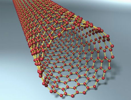
US researchers have demonstrated a form of nanotube archival memory that can store a memory bit for a billion years, and has a theoretical trillion bits/square inch density.
The researchers at the U.S. Department of Energy's Lawrence Berkeley National Laboratory (Berkeley Lab) and the University of California (UC) Berkeley were led by physicist Alex Zettl. They built a prototype device based on a nanoscale iron particle, about 1/50,000th the width of a human hair, moving along a carbon nanotube like a shuttle.
The nano-structure was created in a single step by pyrolysis of ferrocene in argon at 1,000 degreees C. The created nanotube elements are dispersed in isopropanol ultrasonically and deposited on a substrate with electrical contacts applied to the ends of the nanotube. The researchers say these steps are compatible with common semiconductor manufacturing techniques.
By applying an electric current, the iron particle shuttle could be made to move inside the nanotube either away from or towards the current source. When the current was turned off the particle was, as it were, frozen in position. By applying the current in a timed pulse the particle could be made to move a fixed 3nm distance in steps. The speed of movement could be altered by varying the applied bias voltage.
Labels: nano memory, Nano news, nanotech, nanotechnology, nanotechstocks, nanotubes
posted by Ertai @ 6:03 PM
2 comments
MIT has announced a collaboration with the International Iberian Nanotechnology Laboratory in Portugal to create a joint initiative to develop nanotechnology-focused research. Anantha Chandrakasan, director of the MIT Microsystems Technology Laboratories, will serve as MIT’s inaugural director of MIT-INL, along with Carl Thompson, director of the Materials Processing Center.
The MIT-INL initiative will add 10 senior research positions and dedicate $35 million to new research in the program’s first five years at MIT.
According to a joint press release, MIT stands to benefit from INL’s strength in biotechnology, nanotechnology, materials science and engineering. MIT-INL is the first U.S. collaboration for INL, a joint development of Portugal and Spain.
On tap for the first joint projects of MIT-INL are “nanoparticles that can selectively adsorb water contaminants, autonomous microsystems that can move around water supplies and sense contaminants, new materials for energy storage, and revolutionary tools and technologies for monitoring our food supply,” the release reports.
Labels: NANO, Nano news, Nano RD, nanotech, Nanotech stocks, nanotechnology
posted by Ertai @ 5:37 AM
5 comments